- Research
- Open access
- Published:
A PUF-based cryptographic security solution for IoT systems on chip
EURASIP Journal on Wireless Communications and Networking volume 2020, Article number: 231 (2020)
Abstract
The integration of multicore processors and peripherals from multiple intellectual property core providers as hardware components of IoT multiprocessor systems-on-chip (SoC) represents a source of security vulnerabilities for the in-chip communication. This paper describes the concept and the practical results of a SoC security implementation that is illustrative for IoT applications. The mechanism employed in this approach uses physically unclonable functions (PUF) and symmetric cryptography in order to encrypt the transferred messages within the SoC between the microprocessor and its peripherals. The mechanism is experimentally validated at FPGA level, the paper describing also an implementation scenario for an IoT ARM based device.
1 Introduction
1.1 Systems on chip for IoT devices
Internet of Things (IoT) allows objects to be controlled and/or monitored remotely across the existing network infrastructure. A typical IoT system contains several end-point devices that integrate IP cores such as microprocessors, sensors and custom peripherals in order to ensure the communication and computing capabilities for collecting and processing data. The integrated circuits (IC) manufacturers focus on delivering specific solutions for IoT creating more robust and powerful SoCs used in the end-point devices, some designed especially for IoT, like Narrowband IoT (NB-IoT), LoRA, Sigfox [1, 2].
In a typical microprocessor-based system for IoT, the following components are commonly used [3]:
-
Digital system components: a processor (e.g., ARM Cortex-M), bus infrastructure components (AHB and APB), digital peripherals such as I2C/I3C, SPI interfaces, and other optional IP cores like DMA (Direct Memory Access) controllers, crypto engine or true random number generator (TRNG) for communication session keys, as well as secure data storage elements.
-
Memories: Static random access memory (SRAM), non-volatile memory (NVM), for example flash memory, optional boot loader memory, OTP (one-time programmable) memory or mask ROM.
-
Wireless interfaces, radio interfaces
-
Optional analog components.
For exemplification reasons, the Monarch SX SoC designed by Sequans [4] is depicted in Fig. 1, to stress out the increased number of interconnecting IP cores that are part of an IoT element. Based on Sequans’ Monarch LTE-M/NB-IoT module, this SoC includes, besides interfaces and peripherals, specific engines for media processing in audio and voice applications with support for VoLTE on LTE-M, a low-power sensor hub, a GPU and display controller, IoT interfaces for USB, screen, microphone, battery, GNSS, SIM card, Wi-Fi, Bluetooth, keyboard, accelerometer, gyroscope and other sensors.

Different IP cores integrated as part of Monarch SX SoC designed by Sequans [4]
In order to successfully integrate these SoCs into IoT, the applications mandatory characteristics are low cost and minimal consumption. Further application requirements include security, which plays a crucial role in the IoT network and must originate within the endpoint device.
The diversity and increased number of IoT elements and vendors implementing SoC and IP cores combined at the IoT endpoint level (e.g., ARM, Altair Semiconductors, Qualcomm) introduce some specific security breaches and vulnerabilities [5]. Security counter-measures implemented at the software level are not sufficient; a security mechanism should also be considered in the hardware level of the SoC which later will be used in the IoT device. Some of the SoCs include cryptographic IP cores implemented at hardware level which may be responsible for the generation of a public cryptographic key, the decryption/encryption of a message received/sent through the network from another device or network gate.
This paper addresses the security vulnerabilities of IoT SoCs that integrate different IP cores, susceptible to hardware attacks (as described in Sect. 2).
The paper introduces a secure mechanism in order to protect the integrity and privacy of applications and sensitive data from physical attacks.
The proposed cryptographic mechanism introduces two operations, encryption and authentication, that are translated at the SoC level between microprocessor cores and peripherals. The two cryptographic operations use PUF (physical unclonable functions) circuits—their complete implementation and validation is detailed further in this paper.
Inspired by biometrics, PUFs provide a unique way to identify integrated circuits. Comparable in a simplistic way with a “unique fingerprint” of an IC that differentiates one IC from another (though apparently identical), PUFs exploit the inherent variability in integrated circuit manufacturing to implement challenge-response functions whose output depends on the input and on the physical microstructure of the device. Some operations, critical from the security point of view, where PUF could serve as unique identifier as part of the IoT implementation are: authentication, data integrity, access control, privacy [6].
The novelty of the proposed method resides in the use of PUF to enable secure communication in order to counteract security attacks such as: hardware Trojans, snooping bus, malware insertions. The paper proposes an encryption concept to provide secure communication between the components in a SoC in the presence of an untrusted component, which can snoop the data transmitted in the shared bus. The untrusted component may be either a third-party software application or a hardware Trojan. The PUF circuit used for the FPGA experimental prototype, validating the proposed mechanism, is the ring oscillator PUF (RO PUF).
The paper is organized as follows: after describing the security threats for IoT elements and the use cases where the proposed PUF security approach proves to be efficient—also presenting similar work and related industry implementations, the paper focuses on describing the experimental methods used for the implementation of the proposed security mechanism aimed to integrity and privacy in a SoC designed for IoT. Next, the paper describes the implementation and testing results of the PUF-based encryption and authentication mechanism at FPGA level. A discussion follows, analyzing the advantages provided by this implementation. In order to illustrate the applicability of the proposed security method, the practical use-case of the design of an integrated circuit for IoT based on an ARM SoC is also presented, that can be enhanced with PUF-based elements. A comparison with the industry standard ARM TrustZone technology is also presented, as representative for many ARM-based IoT implementations. The last section presents the conclusions.
1.2 Security threats and related work
An Internet-connected device is susceptible to attacks at different levels [7]: (1) communications (man in the middle, weak random number generator, code vulnerabilities); (2) security services (code downgrade, change of ownership or environment, factory oversupply); (3) physical (non-invasive attacks: clock or power glitch, side channel attacks; invasive attacks: package removal—microprobe station); (4) software (buffer overflows; interrupts; malware). The classification of attacks is presented in Fig. 2.

Classification of security attacks
Considering the classification presented above, the following attacks may be thwarted by the introduced method: type 3—physical and type 4—software.
Some examples of typical physical attacks and software attacks, targeted by the security mechanism that we propose, are described in the following.
The necessities of building large SoCs and achieving a good time-to-market force more and more companies to turn to third-party reusable intellectual property [8].
One threat model for SoCs is represented by physical attacks against ICs, which assume the physical investigation of the ICs in order to obtain sensitive information. The physical investigation of an IC refers to exploring parts of the IC which are not available through normal input/output pins. For example, attackers may inspect the IC layout in order to obtain a secret key. These types of attacks are hard to achieve due to high equipment costs. Even so, there are companies specialized in reverse engineering that analyze the circuits and the semiconductor structure of electronic sub-systems, which may lead to disclosure of secrets; one of them is Chipworks. Examples of physical attacks using reverse engineering are presented in [9].
Bus monitoring attacks represent another type of security threats against SoCs. The bus between the processing part and the memory is one of the most vulnerable points in the system: an adversary may easily listen on the bus in order to extract critical information.
Bus monitoring attacks could also reveal access patterns to memories, which may expose sensitive information.
For example, AES implementations use a table of pre-computed values. The order in which the table entries are accessed can reveal secret information [10].
DMA transfers are usually performed during idle times of the bus. A disadvantage of DMA transfers is that they are primarily unsupervised by anti-malware agents. During a DMA transfer, the unsupervised data could be accessed by malicious software which runs on the CPU [11]. After the completion of a DMA activity, the transferred data can be scanned for malicious codes.
A hardware Trojan is a malicious modification of hardware during design or fabrication which causes an IC to have an altered functional behavior, with security consequences. In modern SoCs, cores communicate with each other via a shared bus. Unfortunately, the shared nature of the traditional bus architecture raises several security issues. Malicious cores can obtain secrets by snooping on the bus. In addition, the bus can be used as a covert channel to leak secret data from one core to another. One of the IP cores (for example, the wireless controller) may contain a malicious hardware modification, a Trojan hardware that could leak information and secret keys which are being transferred between peripherals via the bus. Minor modifications to the digital part of a wireless cryptographic chip are enough to leak secret information without altering the far most sensitive analog parts [12]. Nowadays, the SoCs are created using IP cores from third party vendors and only custom peripherals are implemented and tested in house, in order to reduce the cost and to accelerate the time-to-market with minimal engineering resources. The third-party IP cores may contain hardware Trojans which are undetectable through functional verification and physical testing. In a proof-of-concept project, ARM set itself a challenge in 2015 to demonstrate that physical implementation of SoC for an IoT endpoint device is easily attainable for small design groups of companies having almost any size. The design team should rapidly build differentiated solutions by integrating varying combinations of the ARM IP with their own IPs and third-party IPs.
The above-mentioned physical and software attacks could represent threats for IoT subsystems: a malicious person could gain access [13] to a commercial HVAC (heating, ventilation and air conditioning) system, a wireless base station (e.g., for small cells), to implanted medical devices and their controllers, to smart cars and the emerging gateway systems, or to remote industrial sensors.
Though not in focus of the implementation described in this paper, the security mechanism based on PUF circuits may be extended with cryptographic algorithms in order to counteract attacks also from the other two classes mentioned above and represented in Fig. 2: in case of the communication attacks, PUF circuits could generate the secret used in public key cryptography for message exchange. In case of the security issues related to factory oversupply, due to the uniqueness property of PUF circuits an identifier may be generated to uniquely identify each manufactured integrated circuit.
While most of the PUF applications for IoT focus on securing the communication channels with the exterior elements, the proposed implementation is focused on the on-chip communication security. Many IoT security mechanisms have been developed since the discovery of the silicon PUF circuits. Almost all of them address the security attacks from the communication class: authentication between the IoT device and the server, message exchange between IoT devices, physical attacks on memory devices. Some important related work results are resumed below.
The authors of [14] proposed a PUF based mutual authentication protocol between an IoT device equipped with PUFs and a server from a data center. The proposed protocol is immune to cloning attacks because the PUF cannot be reproduced and is immune to physical attacks because the devices do not store any secrets in their memory. A lightweight identity-based cryptosystem is presented in [15] enabling secure authentication and message exchange among IoT devices. The cryptosystem is based on PUF circuits and elliptic curve cryptography. The authors of [16] use RF-fingerprints which are similar to PUF circuits and develop a system architecture that takes advantage of the embedded RF properties of the Tx to authenticate wireless nodes using a machine learning framework in the Rx. An alternative scheme, which is able to solve man-in-the-middle attacks, impersonation attacks and replay attacks, is presented in [17]. The security scheme is based on an efficient key communication agreement phase between two IoT devices. Authenticating IoT devices based on PUF circuits is described in [18]. A RO PUF that uses spatial reconfiguration on an FPGA to provide secure authentication for resource-constrained IoT devices is presented in [19].
Compared to the existing work, our implementation proposal covers the hardware vulnerabilities which can be exploited by software applications or physical investigations of an IoT integrated circuit—more precisely attacks such as: snooping the bus; accessing the sensitive data stored in memories; memory inspection using DMA [20]; copying critical data using DMA reads [20, 21]; hardware Trojans. All these attacks could be achieved with malicious programs gaining access to sensitive data, by exploiting hardware vulnerabilities.
A well-known industrial implementation of IoT security is the ARM TrustZone CryptoCell solution, a comprehensive collection of silicon-proven security modules that provide platform level security services. It provides the system with various cryptographic related services (implementation of symmetric and asymmetric schemes, HASH and keyed HASH functions, random number generation) as well as platform security services required to assure the integrity, authenticity and confidentiality of code and data belonging to different stakeholders (such as OEM, or a service provider to the user) [22]. The security modules provide the encryption and authentication of communication between different devices from the IoT network.
2 Methods/experimental
2.1 Resources used for implementation
The paper proposes and validates experimental an encryption concept to provide secure communication between the components in a SoC, in the presence of an untrusted component that represents a security vulnerability.
The security mechanism is validated through an FPGA (Field-Programmable Gate Array) prototype that shows: (1) the implementation and validation of two security operations (encryption and authentication) at the SoC level between microprocessors and peripherals; (2) the use of PUF secret keys with symmetric cryptographic algorithms which eliminates the requirement of a secure channel in order to transfer the secret key to various IP cores; (3) the analysis of the proposed mechanism in terms of performance and hardware resources.
All implementations were done on Xilinx Virtex 4 FPGA—the XC4VSX35 devices. The tools used in order to construct the prototype are: (1) Xilinx FPGA Editor for manually placing and routing the PUF circuits; (2) Xilinx EDK in order to implement the SoC with the IP cores provided by Xilinx IP catalog; (3) Xilinx SDK for writing the C program which runs on the SoC; (4) Xilinx Project Navigator in order to add the PUF circuits and the required mechanism for generating the secret keys along the SoC; (5) Xilinx Planahead tool for constraining the placement of the SoC IP Cores; (6) ISim Simulator in order to validate the functionality of the applications, to observe the correctness of the encrypted and authenticated transfer and to analyze the latency with the newly introduced cryptographic operations. All of these tools are part of the Xilinx 12.4 Design and Embedded Suite.
In order to show the feasibility of the proposed security concept in real applications, a demonstrator SoC was created with Xilinx IP Cores: a Microblaze microprocessor, a custom cryptographic (crypto) peripheral with two read/write registers and two GPIO (General purpose Input Output) ports configured one as output and one as input. The communication between peripherals inside the SoC was implemented through the Xilinx PLB bus. The result of this system implementation will be presented in Sect. 3. As a use case scenario, it is assumed that sensitive user data are entered into the system on the input port. The critical data is passed to the crypto peripheral and then to the microprocessor, in order to validate the authenticity of the user. In case of validation, the system notifies the user through the output port.
After being completed in Xilinx EDK, the system was imported in Xilinx Project Navigator. Here the 128 RO PUF circuits were added along the system and connected to it. The microprocessor runs a C program which receives the user sensitive data through the GPIO inputs and sends the data to the crypto module for authentication.
In order to analyze the output of the RO PUF, we have collected the results from 30 identical FPGAs—Xilinx Spartan 3E. The results were collected with the help of the software analyzer, Xilinx ChipScope, and their values were compared with each other in order to demonstrate that the sequences are unique. Two binary sequences generated with PUF circuits are different if on average half of the bits differ. The number of different bits between the sequences generated with PUF circuits is named “inter-distance” and is measured using the Hamming distance.
2.2 The concept of the proposed security mechanism
The introduced method aims to analyze and experimentally validate the use of cryptographic-based operations (encryption/decryption, authentication) inside IoT SoCs with minimum costs in terms of hardware resources needed for performance.
The encryption used to secure the data transferred through the internal bus or stored in peripheral registers or in the memory is based on the one-time pad encryption. The one-time pad (the cryptographic key) used for encryption is generated using PUF circuits and Salsa stream cipher. The memory address is involved in one-time pad computation when it comes to secure the stored data. The mechanism is based on the methodology described in the following:
-
(a)
Determining the critical SoC peripherals
-
The IP cores which process sensitive information will own the cryptographic mechanism. The data read or written from the critical IP cores is encrypted.
-
-
(b)
Generating PUF secret keys
-
The secret key is generated using PUF circuits and Salsa 20/20 algorithm. The Salsa 20/20 is a pseudorandom function based on add-rotate-xor operations. The algorithm maps a 256-bit key, a 64-bit nonce, and a 64-bit counter to a 512-bit block of the key stream. The algorithm generates a stream of pseudorandom binary sequences (512 bit blocks) that may be used as encrypted keys for one-time pad encryption.
-
-
(c)
Encryption and decryption
-
Figure 3 shows the general encryption mechanism involving the microprocessor and one peripheral inside a critical domain. The secret key is a pseudorandom key generated with the help of the PUF responses and the pseudorandom stream cipher Salsa 20/20. Both the microprocessor and the peripheral have easy access (direct connections) to PUF responses, and they also have a wrapper which contains the pseudorandom stream cipher Salsa 20/20. The IP core in Fig. 3 is a critical peripheral that processes critical information, so the read and write operations between microprocessor and peripheral registers are encrypted. As both peripherals have direct connections to the output of PUF circuits, there is no need of a secure channel in order to convey a secret key, eliminating the drawback of the symmetric cryptography. The other peripherals that are not allowed to use the critical information do not have access to the PUF circuits nor to the Salsa 20/20 stream cipher. In the same manner, the data written to the system memory or read from the memory may be encrypted using the one-time pad encryption. The memory address will be used by the Salsa 20/20 function (as a 64 bits counter value) in order to generate the same key for the encryption/decryption operations (Fig. 4).
Fig. 3 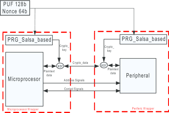
Encryption Scheme between Microprocessor and Peripherals
Fig. 4 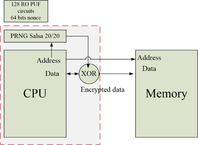
Encryption Scheme between Microprocessor and System memory
-


If the SoC is complex, more critical domains may be considered: each domain contains the peripherals that communicate with each other and each domain will have a unique key generated with PUF circuits.
-
d
Authentication of IP cores
-
This step involves the completion of the wrapper beside the peripherals and the microprocessor with the necessary binary registers in order to authenticate an IP core (marked with dotted line in Fig. 3). The authentication relies on knowing the same pseudorandom key. If two IP cores are allowed to exchange data, their wrappers will generate the same pseudorandom sequences. The microprocessor from one domain may read a mixed bit value of a pseudorandom key and compare it with its one mixed bit value. Confirming the identity of the data source contributes, along the encryption/decryption operations, to counteract the security threats presented in Sect. 2.
-
3 Results
The implementation follows the methodology presented in the previous section. In order to analyze and validate the encryption mechanism, a prototype was implemented on an FPGA element, emulating the hardware design concept that an IoT chip vendor would normally follow in production.
In the implemented application, the communication between the microprocessor and the crypto peripheral—in the system presented in Fig. 5—is encrypted.

System on Chip implemented in Xilinx EDK
The proposed security mechanism assumes that both the microprocessor and the encryption peripheral have an own wrapper for encryption and decryption. In the experimental approach, a coprocessor connected to the microprocessor was used which offers access in detail, needed to add the custom cryptographic wrapper. The encryption peripheral is a custom one, so the encryption wrapper was easily implemented.
The encryption wrappers have access to the hardware area in which the PUF circuits are implemented.
As may be seen in Fig. 5, the Microblaze microprocessor and the crypto peripheral have implemented the security wrapper mechanism. Before sending/receiving data to/from the crypto peripheral, Microblaze encrypts them using an XOR operation with a pseudorandom sequence generated with Salsa 20/20. In this case, the encryption is made using the added coprocessor. On the other part, crypto peripherals decrypt/encrypt the data using the same pseudorandom sequence generated with Salsa 20/20 and bitwise XOR operation.
The sequence of signals described in Fig. 6 shows an encrypted and authenticated transfer: (1) the PLB signals (dplb_m_request, dplb_mrnw, dplb_m_wrdbus, dplb_mwrdack) indicate a master bus request; (2) Microblaze sends the plaintext data (0 × 00000011) to coprocessor (fsl_s_exist, fsl_s_read, fsl_s_data); (3) the coprocessor reads the value, encrypts it using an XOR operation and sends the cryptodata back to Microblaze (fsl_m_data, fsl_m_write); (4) Microblaze performs two serial reads: the authentication value (0 × 22ddbb44) and the cryptotext (0 × 01637ddc); the value of the pseudorandom key is 0 × 01637dc4; (5) Microblaze forwards those two values using two write operations; (6) the PLB signals send those data to the crypto core (m_rnw, m_wrdbus, plb_mwrdbus); (7) the authentication value and the cryptotext reach the peripheral register (user_bus2ip_wrce, slv_reg_write_sel, slv_reg0). The IP core can validate the plaintext data through the authentication value. In the case of disparity, the IP core may alert or stop the microprocessor.

Sequence of signals for an encryption transfer between Microblaze and crypto peripheral
Despite many PUF circuits being presented in the scientific literature, few of them are suitable for FPGA implementations, due to routing complexity and limitations. After analyzing most Silicon circuits, two of them were found to be appropriate for FPGA implementations: the RO PUF (Ring Oscillator PUF) and the Latch-based PUF. In the presented mechanism, the generation of the secret key is based on RO PUF. The RO PUF is based on the structure presented in Fig. 7a, b. It contains 7 inverters connected in a loop which generates a periodical signal. Due to the process variations, the frequencies of the periodical signals will be slightly different. In this way, one of the two counters will reach first the maximum value setting the comparators output to 0 or 1. The result is unpredictable due to the process variations that will modify the signal frequencies. By instantiating more PUF circuits of the same type, a cryptographic key is generated based on process variations and is embedded in the physical FPGA structure.

a RO PUF, b RO PUF on Virtex XC4VSX35
Extracting keys from FPGA-based PUFs using the highly structured nature of modern FPGAs is solution whose feasibility was demonstrated in [23].
One RO PUF circuit is mapped on the hardware resources as in Fig. 7b. This implementation occupies entirely one configurable logic block with 4 slices. Two other 13 bit binary counters and a crossing clock domain circuit are necessary in order to compute one RO PUF answer. The cryptographic key used with Salsa 20/20 involves 128 PUF circuits.
The RO PUF circuits are implemented on the FPGA hardware resources as in Fig. 8, where the occupied area was marked. The hardware resources used to implement the 128 RO PUF circuits, as may be seen in Fig. 7a, b, are presented in Table 1. The main properties of PUF circuits (randomness and uniqueness) were also analyzed in [23, 24]. Our proof-of-concept study considers 30 identical Spartan 3E devices and 4 Spartan 6 devices. The inter-distance histogram (a measure for the uniqueness property) shows that the number of different bits between two sequences generated with PUF circuits is in average, half of the bits (Fig. 9).

RO PUF circuits arranged on FPGA hardware resources

Inter-distance histogram
The critical peripherals that should exchange sensitive data have access to the output of the PUF circuits, the 128 bits generated with RO PUF. The connection is made only once when the chip is implemented and then physically manufactured. All other peripherals from the system cannot access the PUF circuits.
Making the PUF responses available in the peripheral unit will not compromise the security mechanism; the RO PUF key remains tamper-resistant.
Any attempt to disclose the PUF generated key leads to disruption of the IC. Connecting the PUF responses to Salsa 20/20 pseudorandom generator eliminates the requirement of an error correction and detection algorithm in order to obtain stable PUF responses. This application has the advantage to not require stable PUF responses. The oscillating responses help to improve the security level of the mechanism generating different pseudorandom sequences.
The security protocol assumes to adjoin a wrapper that has access to the sequence generated with PUF for one domain and contains a pseudorandom generator. As mentioned above, the chosen pseudorandom generator is Salsa 20/20. The key is generated using 128 PUF circuits, and the value is concatenated two times in order to obtain a 256-bit key. The Salsa 20/20 algorithm computes the pseudorandom value of 512 bits in 21 clock cycles. As shown, it maps a 256-bit key, a 64-bit nonce, and a 64-bit stream position to a 512 bit output. Each block is an independent hash of the key, the nonce, and a 64-bit block number; there is no chaining from one block to the next. The Salsa 20 encryption function is a long chain of three simple operations on 32-bit words: 32-bit additions, 32-bit exclusive-or and constant-distance 32 bit rotation. Salsa 20/20 starts with the initial state, then it first applies the operations for columns and then for rows in 20 repeated cycles, while the final phase adds the initial state to the final result. Salsa 20/20 was chosen as encryption method in our demonstrator due to the fact that it is suitable for a hardware implementation, being based on simple logical operations. In order to experimentally analyze the security concept, each critical peripheral was featured with this wrapper. The implementation of Salsa 20/20 core was made on the Virtex 4 board, and the summary of device utilization may be seen in Table 2. The frequency after synthesis is 139.451 MHz.
The total cycle for transfer and encryption of the data between Microblaze and the custom peripheral is 19 clock cycles. Considering that each of the two operations of reading and writing has this latency of 19 clock cycles, that the encryption and decryption are made combinational (a XOR operation), and that the Salsa 20/20 based on PUF circuits generates the PRG (pseudorandom generator) key in 21 clock cycles, the mechanism from Microblaze and the peripheral are synchronized.
In order to verify the authenticity of the crypto peripheral, the microprocessor could read an authentication value from the crypto peripheral registers and compare it with his own authentication value. In this way, the receiver may verify if the source of data is valid or if the data are compromised. The authentication value is obtained as a mixed process between the bits of the pseudorandom value. Reversing the bits was chosen in order to exemplify the encryption and authentication between the microprocessor and the crypto peripheral.
A more complicated operation may also be used instead of bits reversion.
4 Discussion
4.1 Analysis of the security protocol
The concept presented in the above section aims to counteract the attacks presented in the IoT SoC threat model from Sect. 3. The physical attacks which aim to reveal secret information such as cryptographic keys or sensitive data are counteracted with the newly introduced mechanism. First of all, the cryptographic keys are embedded in the structure of the FPGA/IC and any attempt to disclose their values leads to the disruption of FPGA/IC and implicitly of the SoC or embedded system. This is the most valuable property of PUF circuits and the main advantage compared to a hardcoded key. Moreover, the use of the PUF secret key does not require a transfer of the secret key to the security wrapper; the IP cores have direct connections to PUF responses. Furthermore, the sensitive information is stored as a crypto text inside the memories or local peripheral registers due to the encryption/decryption mechanism.
The bus monitoring or snooping attacks may also be counteracted. Even if an attack leaks sensitive information, the information is encrypted using the pseudorandom generator based on PUF circuits. Practically, it is hard to generate keys with perfect secrecy. This implies that the total length of the generated keys (the space of the keys) must be greater than the total length of the messages (the space of messages). To practically achieve this, a pseudorandom key generator is used. A pseudorandom generation for a class of statistical tests is a deterministic procedure that maps a random seed to a longer pseudorandom string such that no statistical test in the class can distinguish between the output of the generator and the uniform distribution. The PRG used in the implementation, Salsa 20/20, and the seed generated with PUF circuits make it theoretically impossible to decrypt the crypto text captured through bus monitoring. The same explanation is valid for IP cores information leakage due to hardware Trojans insertion or software malicious modifications. Using Salsa 20/20, starting with values generated with PUF circuits, as a pseudorandom generator, the length of the stream cipher is 64 bytes = 512 bits and the length of the messages is 32 bits = 8 bytes as shown above. It is possible to encrypt an equivalent up to 32 GB of messages.
The size of the output space may increase due to oscillating responses of PUF circuits. Temperature or supply voltage variations may affect the response of PUF circuits, leading to the occurrence of instable PUF answers, without affecting the security or performance of the presented protocol. Combining the PUF circuits with a pseudorandom generator eliminates the need for an error correction and detection algorithm. Such algorithms are mathematically complex and require many hardware resources. Also, the PUF responses generate a unique identifier which may be used to uniquely identify an electronic component important for the cyber security or in a cryptographic protocol between different SoCs in order to create a secure communication channel. In the mentioned uses cases (unique identifier; cryptographic protocols), the error correction code should be involved.
With the proposed mechanisms, peripherals can be assigned as “Secure” or “Non-Secure” and the bus system can ensure that the secure peripherals can only be accessed by secure transfers. Also it is possible to have separate memory blocks for secure and non-secure memories. In the secure memory blocks, data will be encrypted in the same manner: the key is generated using the same PRG combined with PUF except that the counter value will be the address of the memory (as seen in Fig. 4). Using the memory address on Salsa 20/20 core function, would allow us to generate the same cryptographic key in both encryption and decryption operations.
The hardware resources required by the SoC along with the PUF circuits and the authentication and communication protocol are: i) the resources required to implement the SoC; ii) the resources required to implement the PUF circuits and the Salsa 20/20 algorithm. For instance, an FPGA, Spartan 3E XC3S500E, which is a low-spec family of FPGAs, has a number of 10,000 equivalent logic gates.
Another low-spec FPGA family is Spartan 6, with the following devices: XC6SLX25 that has a number of 24051 equivalent logic gates; XC6SLX45—43661; XC6SLX75—74637; XC6SLX100—101261; XC6SLX150—147443. The high-end FPGA families Virtex, Spartan 7 or Artix 7 have even more hardware resources. All of these FPGAs have the necessary hardware resources in order to implement a SoC with the presented security mechanism. The instances of RO PUF circuits required a number about 2500 equivalent logic gates. However, nowadays, a fundamental trade-off between speed, frequency and security begins to appear. The system architect has to find an optimal solution for a SoC that will run at high speed, will require optimal hardware resources and will be also secure. The tradeoff is tightly correlated with the goal of the final application. Analyzing the implemented system, there are 40 clock cycles from the moment in which the data are encrypted by the coprocessor until the moment that data arrive at the register of the IP core. The pseudorandom sequence of the IP core is delayed by 20 clock cycles in order to synchronize the pseudorandom secret key generator between the microprocessor and the IP cores. Typically, a transfer on the PLB bus takes around 5–6 cycles, while an encrypted and authenticated transfer takes 40 clock cycles. This means that the total execution time of the SoC will increase about 8 times.
where Ninstruction is the number of instructions for a software program; Ncycle per instruction is the number of clock cycles for one instruction, and Tcycle is the duration time [ns] for one cycle.
Considering the encrypted transfer of data: if the number of clock cycles is increased 8 times (40 clock cycles/5 clock cycles = 8), then the overall execution time of a software program will also increase 8 times.
However, this increase will not drastically affect the overall SoC performance due to the higher working frequency of SoC and due to the hardware implementation of the security mechanism. If the frequency is high enough, an increase in the number of clock cycles may be acceptable.
In the formula presented above, if the number of cycles per instruction will increase and the frequency will increase enough (for example 8 times), the overall execution time of a program will remain the same. With a higher frequency, the difference between the execution time of a program with encryption mechanism and the default execution time could be minimized.
where \(T1_{{{\text{cycle}}}} = \frac{1}{{n*f_{{{\text{clk}}}} }}\) is the increased frequency of the microprocessor.
A security protocol implemented at the hardware level may avoid many software and hardware security attacks: the software programs are composed of high-level instructions (e.g., C/C++), and the high-level instructions are compiled by a compiler and result into assembly language instructions specific to each microprocessor; the assembly language instructions are translated into machine (binary) language instructions. The interpretation of these binary instructions is achieved in hardware by the logic gates implemented in CMOS technology.
4.2 The use-case of a security mechanism for an ARM IoT subsystem
Available for licensing now, the ARM IoT subsystem can be combined with other ARM building blocks such as Cortex-M processor cores and Cordio wireless interfaces to form the basics of a complete chip design [26]. This means that a new security protocol could be easily implemented in the ARM IoT subsystems.
A simple example of SoC for IoT applications is presented in Fig. 10. The system was obtained as a result of the ARM challenge set in 2015 [26]. The specific task was to rapidly implement this prototype silicon demonstrator platform—called Beetle—with only three engineers and in less than three months. The resulting platform integrates ARM IP on a single piece of silicon and includes an IoT subsystem [27] with Cortex-M microprocessor, Bluetooth ‘Smart’ Low-Energy (BLE) radio, plus embedded flash memory.

ARM-based IOT System on Chip [28]
As may be seen in this figure, third-party communication IP cores (Quad SPI, 2Xspi, 2xI2C, DMA, Wifi Radio) are involved in the design. These IPs are serial interfaces that may be used to communicate with wearables’ sensors or SoCs and have access to the AHB interconnect. One of these third-party IP cores may be used to leak out of the chip sensitive information.
Sensitive information may be for example decryption of the data acquired from an intelligent sensor or cryptographic passwords. Some attack scenarios may be identified: the I2CWifi Radio interface may have a hardware Trojan that listens on the AHB interconnect and send the sensitive information on network to the second SoCs. Without a security mechanism, software applications may snoop on the bus or on the I/O Memory or use DMA transfers in order to obtain sensitive information. The sensitive information may be sent outside the IoT subsystem on the network. Software applications may configure the DMA to get sensitive data from memory areas in which they do not have access rights.
The proposed mechanism supposes that the information is transferred encrypted on the AHB interconnect. For example, the Cortex microprocessor will communicate through encrypted messages with the radio IP core or other IP cores involved in the computation of sensitive information. The encryptions are made with different keys. If the encrypted messages are intercepted, it is impossible to compute the plain-text data or the cryptographic key due to the cryptographic keys generated with PUF circuits and Salsa pseudorandom generator.
The proposed mechanism may easily join the ARM SoC. The PUF circuits are implemented on a part of the silicon die, whereas the encryption wrapper may be added to the IP cores, connected on the data interface.
We have analyzed the possibility to integrate the security encryption wrapper composed of PUF circuits and Salsa PRG on the ARM 3 Cortex design start evaluation system provided by ARM. Cortex-M3 DesignStart Eval provides developers with an easy way to develop and simulate SoC designs based on the ARM Cortex-M3 processor. The ARM 3 Cortex design is presented in Fig. 11 [29].

ARM 3 Cortex DesignStart Eval
The RTL design was simulated using an obfuscated RTL version of Cortex M3 processor. Even with the obfuscated RTL, we have access to processor interface used to transfer data on the AHB interface. In this way, the presence of a coprocessor responsible with cryptographic operations is no longer required. On our simulation, the Cortex M3 runs a C program that is testing the GPIO0 write access.
Figure 12 presents a transfer on AHB bus from Cortex ARM3 to GPIO0 write registers. The transfer takes 3 clock cycles from the moment when the microprocessor sets the peripheral address on HADDRS bus, until data arrives in the GPIO0 register.

ARM 3 Cortex and GPIO0 RTL simulation
The transfer size is 32 bits. Considering Fig. 12, the master signals used in a write transfer are: (1) HADDRS: the 32 system address bus; (2) HWRITES indicates the transfer direction; when HIGH, this signal indicates a write transfer, and when LOW, a read transfer; (3) HSIZES indicates the size of the transfer, that is typically byte, halfword or word; (4) PRNG indicates the pseudo random key generated for encryption; (5) HWDATAS: the write data bus transfers data from the master to the slave during write operation; (6) hwdatas_PRNG represents the encrypted data with an XOR between the HWDATAS and PRNG value. Slave signals used in a data transfer are: (1) HADDR, (2) HSEL, (3) HWDATA and (4) HWRITE with the same meaning as in the case of master signals. The HSEL signal is a combinatorial decode of the address bus [30].
The encryption mechanism assumes that both the ARM 3 Cortex and the GPIO peripheral have an instance of Salsa 20/20 which accesses the PUF circuits. The two instances of Salsa 20/20 are synchronized on the AHB clock and generate 512 bits at each 21 clock cycles. The 512 bits pseudo random generated value may be divided in chunks of 32 bits that are used to encrypt data on consecutive transfers. A transfer takes 3 clock cycles. On the master side, the value of HWDATA may be encrypted using a simple XOR operation with a chunk of 32 bits from the total 512 bit generated with Salsa 20/20. In the same way, the value received on HWDATA could be decrypted using an XOR operation with a chunk of 32 bits from the total 512 bit generated with Salsa 20/20.
The same mechanism may be used with more complex peripherals.
There are many suppliers of peripherals based on AHB and APB protocols. Designers might also reuse existing peripherals from a previous design based on legacy processor architectures. The IP core may be modified by the designer in order to connect to the encryption wrapper.
The ARM TrustZone Technology offers hardware-isolation for trusted software. It can be used with a Cortex-A processor, and recently, it is supported in the latest Cortex-M23 and Cortex-M33 [31]. In this paper, the proposed method creates an addition mechanism that may help a SoC used in IoT applications to secure the sensitive information. The advantages of using PUF circuits are that the generated binary sequence may be used to uniquely identify the chip or may be involved as well in communication protocols among IoT devices and servers. Also the encryption could be used in ICs that are based on other processors than ARM or on MPSoC (multiprocessor system on chip) with more than one microprocessor in a SoC [32]. In the ARM-based architectures, the mechanism may be used in conjunction with the ARM TrustZone Technology.
The concept of ARM TrustZone Technology is based on peripheral isolation. Some relevant examples of ARM TrustZone components are [33]:
-
A memory protection controller for partitioning of a memory block into Secure and Non-Secure spaces
-
A peripheral Protection Controller for assigning peripherals into Secure and Non-Secure domains
-
Bus security wrappers useful for legacy bus masters.
5 Conclusion
The paper presents a security concept for a complex SoC with more than one microprocessor and validates experimentally its significant benefits through an illustrative implementation of cryptographic operations. The paper shows (1) the implementation of RO PUF circuits and how they are to be used along the Salsa 20/20 algorithm in order to create a pseudo random generator and (2) how to use symmetric encryption inside a System on Chip based on two different microprocessors: Microblaze and ARM.
The aim of the proposed mechanism is to contribute to the overall IoT security. While most of IoT security concepts address the communication between IoT elements, the proposed mechanism targets the security on the communication between the IP cores inside an IoT SoC. The hardware implementation proposed in the paper can easily be extended to accommodate more complex SoCs with an increased number of peripherals and interfaces, including IoT-specific radio IP cores.
The cryptographic operations (encryption/decryption and authentication) are based on a pseudorandom generator composed of PUF secret keys and the Salsa 20/20 algorithm. The advantages of using a PUF secret key instead of a hardcode key are: (1) all the IP cores inside a domain have access to the PUF responses through direct connections, eliminating the requirement of a secure channel in order to share a secret key; (2) the PUF circuits may be used to create an unique identifier for the physical circuit and may be used against security attacks like counterfeiting, cloning integrated circuits, stealing IP cores or software applications, and (3) the PUF circuits are tamper-resistant, which means that any direct contact to the physical device will destroy the original PUF secret key.
Cryptographic security primitives by themselves are not enough to guarantee security, since the mobile computing devices and IoT devices are open to other threats such as physical attacks and hardware Trojans. The method presented in this paper uses symmetric key algorithms in order to thwart some security issues of the SoCs. Considering other research results reported in this field, it can be stated that this encryption/decryption mechanism is introduced for the first time at the SoC level, between the IP cores. Adding the PUF circuits at the core of a PRG increases the randomness in the generator.
The experimental results show that the performance/speed of symmetric key algorithms may be used to construct a security mechanism at hardware level between the IP cores.
As an increased number of IoT devices are based on ARM SoCs, the paper also presents a proof-of-concept use case for the security mechanism, implemented for ARM IoT elements, as well as a comparison with the ARM TrustZone industry standard technology.
System-on-Chip security is a mandatory requirement, even if not sufficient, for the security of IoT end devices, facing the challenge for the Cloud “hardware as a service” of tomorrow.
Availability of data and materials
The datasets used and/or analyzed during the current study are available from the corresponding author on reasonable request.
Abbreviations
- AHB:
-
Advanced high performance
- APB:
-
Advanced peripheral bus
- DMA:
-
Direct memory access
- FPGA:
-
Field programmable gate array
- IC:
-
Integrated circuit
- IP Cores:
-
Intellectual property cores
- I2C:
-
Inter-integrated circuit—serial interface
- NVM:
-
Non-volatile memory
- OTP:
-
One-time programming
- PUF:
-
Physical unclonable function
- SoC:
-
System on chip
- SPI:
-
Serial peripheral interface
- SRAM:
-
Static random access memory
- TRNG:
-
True random number generator
References
R. Sharan Sinha, Y. Wei, S. Hwang, A survey on LPWA technology: LoRa and NB-IoT. ICT Express 3(1), 14–21 (2017)
B. Vejlgaard, M. Lauridsen, H. Nguyen, I.Z. Kovacs, P. Mogensen, M. Sorensen, Coverage and capacity analysis of Sigfox, LoRa, GPRS, and NB-IoT, in 2017 IEEE 85th Vehicular Technology Conference (VTC Spring), Sydney, NSW, pp. 1–5.
J. Yiu, Designing a System-on-Chip (SoC) with an ARM Cortex-M processor. A starter guide. ARM Whitepaper (2017)
Sequans Communications S.A., Sequans Introduces Monarch SX: LTE-M/NB-IoT System-on-Chip for Integrated IoT Devices. Press Release. https://www.sequans.com/wp-content/uploads/2018/08/PI-Monarch-SX-5-20180807.pdf. Accessed Dec 2018
M. Ammar, G. Russello, B. Crispo, Internet of Things: a survey on the security of IoT frameworks. J. Inf. Secur. Appl. 38, 8–27 (2018)
R. Maes, I. Verbauwhede, Physically unclonable functions: a study on the state of the art and future research directions, in Towards Hardware-Intrinsic Security. Information Security and Cryptography. ed. by A.R. Sadeghi, D. Naccache (Springer, Berlin, 2010)
Y. Yang, L. Wu, G. Yin, L. Li, H. Zhao, A survey on security and privacy issues in Internet-of-Things. IEEE Internet Things J. 4(5), 1250–1258 (2017)
M. Rihani, M. Mroue, J. Prévotet, F. Nouvel, Y. Mohanna, ARM-FPGA-based platform for reconfigurable wireless communication systems using partial reconfiguration. J. Embed. Syst. 2017, 35 (2017)
A. Waksman, S. Sethumadhavan, J. Eum, Practical, lightweight secure inclusion of third-party intellectual property. IEEE Des. Test 30(2), 8–16 (2013)
P. Colp, J. Zhang, J. Gleeson, S. Suneja, E. de Lara, H. Raj, Protecting data on smartphones and tablets from memory attacks, in ACM International Conference on Architectural Support for Programmning Languages and Operating Systems (2015)
M. Eckert, I. Podebrad, B. Klauer, Hardware Based Security Enhanced Direct Memory Access, Communications and Multimedia Security, Volume 8099 of Lecture Notes in Computer Science (Springer, Berlin, 2013), pp. 145–151
Y. Jin, Y. Makris, Hardware trojans in wireless cryptographics ICs. IEEE Design Test Comput. (2010)
R. Newell, The Biggest Security Threats Facing Embedded Designers, Electronic Design (2016). https://www.electronicdesign.com/iot/biggest-security-threats-facing-embedded-designers. Accessed Dec 2018
A.M. Naveed., K.C. Chua, B. Sikdar, Physical unclonable functions for IoT security, in Proceedings of the 2nd ACM International Workshop on IoT Privacy, Trust, and Security (2016)
U. Chatterjee, R. S. Chakraborty, D. Mukhopadhyay, A PUF-Based Secure Communication Protocol for IoT. ACM Trans. Embed. Comput. Syst. 16, 3, Article 67, 25 (2017). https://doi.org/10.1145/3005715
B. Chatterjee, D. Das, S. Sen, RF-PUF: IoT security enhancement through authentication of wireless nodes using in-situ machine learning, in 2018 IEEE International Symposium on Hardware Oriented Security and Trust (HOST) (2018), pp. 205–208
A. Braeken, PUF based authentication protocol for IoT. Symmetry 10, 352 (2018). https://doi.org/10.3390/sym10080352
M. Barbareschi, P. Bagnasco, A. Mazzeo, Authenticating IoT devices with physically unclonable functions models, in 10th International Conference on P2P, Parallel, Grid, Cloud and Internet Computing (3PGCIC), Krakow, pp. 563–567 (2015)
C. Marchand, L. Bossuet, U. Mureddu, N. Bochard, A. Cherkaoui, V. Fischer, Implementation and characterization of a physical unclonable function for IoT: a case study with the TERO-PUF. IEEE Trans. Comput. Aided Des. Integr. Circuits Syst. 37(1), 97–109 (2018)
P. Stewin, Detecting Peripheral-Based Attacks on the Host Memory (Springer, Berlin, 2015)
A. Huang, Keeping Secrets in Hardware: The Microsoft Xbox Case Study (MIT, Cambridge, 2002)
ARM Developer, Trust Zone Cryptocell (2017). https://developer.arm.com/products/system-ip/security-ip. Accessed Dec 2018
A. Stanciu, M. Cirstea, F. Moldoveanu, Analysis and evaluation of PUF-based SoC designs for security applications. IEEE Trans. Ind. Electron. 63(9), 5699–5708 (2016)
A. Babaei, G. Schiele, Spatial reconfigurable physical unclonable functions for the Internet of Things, in Security, Privacy, and Anonymity in Computation, Communication, and Storage. SpaCCS 2017. Lecture Notes in Computer Science, vol 10658, ed. by G. Wang, M. Atiquzzaman, Z. Yan, K.K. Choo.
D. Robinson, ARM details on-chip subsystem to ease development of IoT silicon. https://www.v3.co.uk/v3-uk/news/2411007/arm-details-on-chip-subsystem-to-ease-development-of-iot-silicon. Accessed Dec 2018
J. Yoshida, Cellular IoT Chip Battle Escalates at MWC, in EE Times (2017).
L. Jalal, V. Popescu, M. Murroni, IoT architecture for multisensorial media, in 2017 IEEE URUCON, Montevideo, pp. 1–4
Breker ARM-based SoC Verification. https://brekersystems.com/products/armv8/. Accessed Dec 2018
ARM 3 Cortex DesignStart Evaluation. https://developer.arm.com/products/designstart. Accessed Dec 2018
AMBA 3 AHB Lite Protocol. https://www.eecs.umich.edu/courses/eecs373/readings/ARM_IHI0033A_AMBA_AHB-Lite_SPEC.pdf. Accessed Dec 2018
T. Whitfield, Implementing an IoT end-point SoC platform, in EE Times Europe (2016). https://www.eenewseurope.com/archives/pdf-eete-feb-2016.pdf. Accessed Dec 2018
J. Yiu, Enhanced Security and Energy Efficiency of Microcontrollers and SoCs, in EmbeddedWorld 2016 Exhibition &Conference
Introducing ARM TrustZone. https://developer.arm.com/technologies/trustzone. Accessed Dec 2018
Acknowledgements
The authors would like to thank the members of the COST Action CA15104 IRACON, “Inclusive Radio Communication Networks for 5G and Beyond,” for their valuable advice and guidance related to the concepts presented in this paper.
Funding
Part of the research presented in this paper was supported by the Sectoral Operational Programme Human Resources Development (SOP HRD), ID137070 financed from the European Social Fund and by the Romanian Government.
Author information
Authors and Affiliations
Contributions
AS has the main contribution for the security mechanism concept and was responsible for developing the PUF security mechanism in FPGA. TB was responsible for investigating the security mechanisms that are suitable to be implemented, the implementation of the pseudorandom generator mechanism and has authored the manuscript in relation to the IoT security threads. MC has contributed to the security mechanism concept and was responsible for the analysis and interpretation of data resulted from the implementation, as well as suggesting other relevant use-cases for the PUF based testing. FS has contributed to the FPGA implementation environment selection and setup and was responsible for drafting the manuscript and revising it critically. All authors read and approved the final manuscript.
Corresponding author
Ethics declarations
Competing interests
The authors declare that they have no competing interests.
Additional information
Publisher's Note
Springer Nature remains neutral with regard to jurisdictional claims in published maps and institutional affiliations.
Rights and permissions
Open Access This article is licensed under a Creative Commons Attribution 4.0 International License, which permits use, sharing, adaptation, distribution and reproduction in any medium or format, as long as you give appropriate credit to the original author(s) and the source, provide a link to the Creative Commons licence, and indicate if changes were made. The images or other third party material in this article are included in the article's Creative Commons licence, unless indicated otherwise in a credit line to the material. If material is not included in the article's Creative Commons licence and your intended use is not permitted by statutory regulation or exceeds the permitted use, you will need to obtain permission directly from the copyright holder. To view a copy of this licence, visit http://creativecommons.org/licenses/by/4.0/.
About this article

Cite this article
Balan, A., Balan, T., Cirstea, M. et al. A PUF-based cryptographic security solution for IoT systems on chip. J Wireless Com Network 2020, 231 (2020). https://doi.org/10.1186/s13638-020-01839-6
Received:
Accepted:
Published:
DOI: https://doi.org/10.1186/s13638-020-01839-6