- Research Article
- Open access
- Published:
A Programmable, Scalable-Throughput Interleaver
EURASIP Journal on Wireless Communications and Networking volume 2010, Article number: 513104 (2010)
Abstract
The interleaver stages of digital communication standards show a surprisingly large variation in throughput, state sizes, and permutation functions. Furthermore, data rates for 4G standards such as LTE-Advanced will exceed typical baseband clock frequencies of handheld devices. Multistream operation for Software Defined Radio and iterative decoding algorithms will call for ever higher interleave data rates. Our interleave machine is built around 8 single-port SRAM banks and can be programmed to generate up to 8 addresses every clock cycle. The scalable architecture combines SIMD and VLIW concepts with an efficient resolution of bank conflicts. A wide range of cellular, connectivity, and broadcast interleavers have been mapped on this machine, with throughputs up to more than 0.5 Gsymbol/second. Although it was designed for channel interleaving, the application domain of the interleaver extends also to Turbo interleaving. The presented configuration of the architecture is designed as a part of a programmable outer receiver on a prototype board. It offers (near) universal programmability to enable the implementation of new interleavers. The interleaver measures 2.09 m in 65 nm CMOS (including memories) and proves functional on silicon.
1. Introduction
With the multitude of digital communication standards in use nowadays, a single device must support an increasing number of them. Think for instance of a mobile phone that is required to support UMTS, DVB-H, and 802.11 g. Moreover, these radio standards are rapidly evolving, leading to constant (re)design of solutions. Accordingly, the concept of Software-Defined Radio [1] is becoming more and more attractive. The aim of SDR is to provide a single platform consisting of a hardware layer and a number of software layers on which a set of radios from different communication standards can run as software entities in parallel. Next to microprocessors and DSPs, the hardware layer will contain a number of (programmable) accelerators for high-speed baseband processing (e.g., programmable channel decoders). This paper focusses on the design and implementation of a scalable-throughput programmable channel interleaver architecture. Interleaving is a support operation for channel decoding. It dramatically improves the channel decoder performance by breaking correlations among received neighboring symbols in the frequency or time domain. A channel interleaver for Software-Defined Radio has to support multiple interleaving functions. The total required throughput depends on the use cases that have to be supported. To offer a matching solution for a set of use cases, the programmable channel interleaver is designed to be scalable in throughput.
The paper is structured as follows: Section 2 describes the requirements for the architecture, Section 3 gives a top-down description of the architecture design, Section 4 describes the considerations for mapping interleavers to the architecture, Section 5 discusses the results of simulations for a large number of interleaving functions and implementation of the architecture, and Section 6 gives an overview and detailed comparison with the previous work [2–4]. At this point we already note that existing multistandard interleavers target a specific set of standards, whereas we aim at a truly programmable architecture.
2. Requirements
2.1. Interleavers for Wireless Communication
An Interleaver for wireless communication typically performs a fixed permutation on a block of symbols. Symbols can be hard bits or soft bits, where soft bits typically have a precision of 4–6 bits, and block sizes vary from hundreds to thousands of symbols. Communication standards often support multiple block sizes, up to hundreds. So-called block interleavers have no residual state between the processing of successive blocks. In contrast, so-called convolutional interleavers perform a permutation across block boundaries, and may require much larger memories to store their state ((e.g., over 200 MB for DVB-SH), see Table 1). For some interleavers, the permutation is not specified on individual symbols, but on pairs of symbols or even larger units ("granularity" in Table 1).
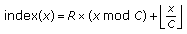
The permutation functions applied in todays communication standards show a surprisingly large variation. An example of a simple permutation,  , is matrix transposition; the exchange of rows and columns:

where  is the index in the interleaved block (ranging from 0 to
  ), the constants
  and
and  represent the two dimensions of the matrix, and the block size equals
  . A typical complication is that the columns are permuted as well, for example, according to a bit reversal scheme.
In other permutations, addresses are based on Linear Feedback Shift Registers (LFSR). In refinements of this scheme, the LFSR addresses are clipped within the range specified by the block size.
Yet another class of permutation schemes is based on an array of FIFOs, where the FIFO sizes increase linearly with their position in the array. An example of a less regular variation of this theme, is the DVB-SH fifo-based time interleaver with arbitrary lengths.
An example of an interleaving function with a large state size and a small interleaving granularity is the time interleaver for DAB. Because of its size (approximately 0.5 MB) the time interleaver state has to be stored in some off-chip memory. Interleaving is then performed on sub-blocks which should be read from and written to the external memory in a smart way.
Even for a single standard, it is common to have two or more interleave stages, typically of a very different nature.
2.2. Requirements
Our goal is an architecture for an interleaver machine that supports this large variation in permutation functions for a wide range of digital communication standards. More specifically, the interleaver machine
-
(i)
must be programmable for interleavers in today's digital communication standards in the consumer space: cellular, connectivity, and broadcast,
-
(ii)
must be scalable in throughput to allow the derivation of hardware versions for lower and higher throughput use cases,
-
(iii)
must provide a gross throughput of 0.5G symbols/s to 1G symbols/s for the prototype board,
-
(iv)
must allow a low-cost implementation; specifically, hardware costs for address calculations must be small compared to the costs of the intrinsically required memory; furthermore, for standards with a large interleaver state size it must be possible to use (cheaper) off-chip memories,
-
(v)
must support run-time loading of different permutation functions,
-
(vi)
must support multiple streams simultaneously by serving them block by block.
The requirement of 1G symbols/s may seem excessive, but several trends suggest even higher needs like the following:
-
(i)
4G standards and beyond hint towards 1G symbols/s down-link data rates,
-
(ii)
the desire to have multistream scenarios with even more demanding combinations of digital communication standards (e.g., connectivity and 4
 DVB-T),
 -
(iii)
the use of iterative decoding schemes [14] including iterative channel (de)interleaving.
 DVB-T),
The amount of memory required to store the state of the interleaver machine and the required throughput depend on the set of standards to be supported. Accordingly, we aim at a scalable architecture.
3. Architecture
We solve interleaving by writing the data in a certain order (i.e., an access sequence) to a memory and by reading it out in a different order. For this we require random access to a memory on a soft-bit granularity. Soft-bit precision typically ranges from 4 to 6 bits. Choosing an 8-bit word size instead of 6 bit makes little difference in cost and allows the architecture to support byte interleavers (such as DVB-T Outer interleaving) efficiently.
Storing the interleaver state is expensive for an interleaving function with a large state size like DVB-SH Time and DAB Time. Fortunately interleaving is defined for those cases either on a coarse granularity or on a block-level composable fine granularity. This allows storage of state for large interleaving functions in a cheaper off-chip memory.
To support sufficient flexibility for both the external and the local memory, we use a single, programmable address generator. For the majority of the studied interleaving functions the associated address sequences can be expressed in a 16-bit address space. The interleaving functions with large state on the other hand require a 32-bit address space. For coarse-grained 32-bit interleaving functions that require no further fine grained interleaving, the programmable channel interleaver allows a bypass around its local memory in the so-called transfer mode.
To facilitate multistream, the architecture makes use of offsets for both the address generator program memory and the interleaving data memories. This allows multiple address generation programs or data blocks to be stored in the memories simultaneously. Based on the relevant use cases, the first implementation of the programmable channel interleaver features 1 Mbit of local data memory and 256 kbit of address generation program memory.
For cost efficiency, single-port SRAMs are used. Hence, for each soft bit we require a write and read cycle. For a use case that requires a total throughput in the range of 0.5 to 1 giga soft bit per second, this implies memory access rate of up to 2 GHz. The architecture needs to operate at a much lower frequency to be power efficient. This leads to a multibank solution for the data memory featuring 8 memory banks running at 250 MHz for our prototype.
The required throughput is close to  the memory bandwidth. Accordingly, it requires 8 addresses per clock cycle to be generated. Given the nature of interleaving functions, it is unlikely that those 8 addresses are all destined for different memory banks and will therefore lead to bank conflicts. To obtain the high throughputs required by the use cases, we cannot afford a lot of throughput loss due to these bank conflicts. Given the large variety in interleaving functions, a generic approach to resolve bank conflicts is required.
To allow a fitting hardware solution for lower or higher throughput use cases, the architecture is designed to be scalable in its processing parallelism  , where
  is a power of 2. For our prototype
  is chosen equal to 8.
The following sections describe our solution for a programmable channel interleaver architecture featuring a programmable vector address generator and a multibank memory with conflict resolution. First the top-level architecture is described, followed by a more detailed description of the vector address generator and the multibank memory.
3.1. Top Level
The interleaver architecture consists of a vector address generator (iVAG), a conflict resolving memory (CRM), three interface controllers, and a main controller. Figure 1 depicts the top-level architecture in terms of its main components and their connections. Control flows are indicated by dashed arrows and data flows by solid arrows. Both the iVAG and the CRM are scalable in their parallelism  , as is indicated in Figure 1. The interleaver can perform tasks of the types mentioned in Table 2. The interleaver is configured by an external
  controller via the APB (Advanced Peripheral Bus) by storing the configuration data for a certain set of maximally two tasks in one of the register sets in the APB controller. After configuration, the
  controller will kick off the main controller. Based on the configuration stored in the APB registers, the main controller controls all actions and data streams within the interleaver in accordance with the configured set of tasks. When the main controller has finished all operations for the current set of tasks it will indicate this to the
  controller. The
  controller can then reconfigure the interleaver for another set of tasks. To lower the
  controller involvement, the main controller can be programmed for a number of repetitions of the set of tasks. A typical example of a set of tasks is the alternation of a Input Data task and an Output Data task.

Interleaver architecture Top level.
To support multistream scenarios, the  controller has to take care of the scheduling of block processing for the different streams. Depending on the latency constraints of the standards, there are two options:
-
(i)
Block-by-block processing controlled by the
 controller. This is preferred when the interleaving block processing times fit well within the latency constraints for the different streams.
 -
(ii)
If the latency constraint of a stream does not allow the scheduling of an interleaving block of another stream, the iVAG programs for this other stream can be rewritten to process partial interleaving blocks. The iVAG allows storage of the state of an address generation program so that it can continue with the same address sequence in a subsequent run.
 controller. This is preferred when the interleaving block processing times fit well within the latency constraints for the different streams.
When we assume that the programs are loaded in the iVAG program memory, the reconfiguration of the interleaver can be done in typically 5 to 10 cycles, depending on the number of parameters that need to be communicated (configured via the APB by the  controller).
The interleaver has two DTL (Device Transaction Level [15]) data I/O ports. The DTL-MMBD (DTL Memory-Mapped Block Data) port is a bidirectional interface that allows a block of data to be retrieved from or stored to a location indicated by a 32-bit address. The DTL-PPSD (DTL Peer-to-Peer Streaming Data) port is a unidirectional interface that streams data from the interleaver to an external target.
Prior to any interleaving the program data is copied into the iVAG memory via the DTL-MMBD port (task: Program Load). The iVAG memory can contain multiple programs. A program is selected by configuring an offset in the iVAG memory. After Program Load the interleaver is ready to process data. There are three distinct modes of operation. The Input Data tasks retrieve data via the DTL-MMBD port from an external source and store this data in the CRM using vectors of addresses from the iVAG. The Output Data tasks retrieve data from the CRM using vectors of addresses from the iVAG and send this data to an external target. The data is either output block-based via the DTL-MMBD port or stream-based via the DTL-PPSD The Transfer tasks retrieve data from an external source and directly send this data to an external target.
For most of the task types the source of the 32-bit address(es) used by the DTL-MMBD port can be chosen. The two options are the APB controller and the iVAG. If the APB controller is the source it provides a single fixed 32-bit address that was configured by the  controller. The iVAG provides, depending on the program, one or multiple 32-bit addresses with a maximum of 64. These are buffered in the DTL-MMBD controller and used for subsequent transfers.
3.2. Conflict Resolving Memory
Research on vector access performance for multibank memories has a long history. In [16] a memory system was proposed with input and output buffers for all memory banks including a stalling mechanism and a bank assignment function based on a cyclic permutation.
Also in the field of Turbo interleavers good progress has been made towards parallel architectures. Solutions making use of buffers and a bank assignment system somewhat similar to [16] were adopted. Much effort went into the optimization of the bank assignment function implementation [17–19]. However, for these solutions buffer sizes were determined for a fixed set of interleaver parameters and functions. In [20] the usage of flow control (stalling mechanism) was proposed to optimize for a more general average case. In [21] this was followed up with an analysis of deadlock free routing for interleaving with flow control. We propose a run-time conflict-resolution scheme in order to support the large variety of permutations, including permutations not known at the hardware design time.
The CRM (Figure 2) comprises  memory banks, where
  is a power of 2, and can process up to 1 vector of
  independent memory accesses per clock cycle. The concept is similar to what was proposed by [16]. By means of a crossbar network (Bank Sorting Network) the accesses of a vector are routed to the correct memory banks. A conflict occurs when multiple accesses within a vector refer to the same memory bank. Each memory bank has its own Access Queue in which conflicting accesses are buffered. All Access Queues have depth
  . Note that this is the minimum size with a processing granularity of vectors of
  accesses. When an Access Queue cannot accept all of its accesses, none of the Access Queues will accept accesses during that cycle. The CRM will therefore stall the iVAG. A memory bank will process accesses as long as their Access Queue is not empty and the CRM itself is not stalled by a receiving interface controller.

Conflict resolving memory.
In the case of read accesses, the memory banks will retrieve and output data. To restore this data to the original order of the accesses, the output data of each bank needs to be buffered in Reorder Queues and subsequently be restored to its original order by the Element Selection Network. Each Reorder Queue has a depth of  , equal to Access Queue depth.
The conflict resolution system is based on the observation that for interleaving functions every bank is accessed the same number of times on average for each interleaving block. Bank conflicts are spread over time by the queues. Inherent to this solution is that only a certain local density of conflicts for each individual bank can be handled efficiently. When long bursts of conflicts occur for a particular bank, the conflict resolution system becomes ineffective. To counteract this efficiency degradation, the bank assignment function of the Bank Sorting Network features an optional permutation:

where  represents a local address on a memory bank,
  the memory bank index,
  the new permuted memory bank index
  (e.g.,
  for 16-bit addresses and
  ).
).
This permutation can be highly effective in spreading the accesses more evenly over the  banks. A good example is the matrix interleaver defined in (1). Assume
  ,
, , and
, and  . The input data block is written linearly to the memory banks in vectors of four
  pairs as is shown in Table 3. The mapping of interleaving block indices to
  pairs is defined by

where  represents a local address on a memory bank,
  the memory bank index, and
  the index in the interleaving block. When linearly accessing the memory, all accesses are spread perfectly uniformly over the banks. The data block is read out in an interleaved order as shown in Table 4.
When  is a divider of
  , there will be bursts of
  bank conflicts. For large values of
  this leads to a CRM efficiency close to
  . When the optional permutation is used for this example, writing is performed as shown in Table 5. During the otherwise troublesome reading process, the conflict bursts are now broken and a uniform distribution over the banks is obtained as can be seen from Table 6.
3.3. Interleaver Vector Address Generator
During a study of solutions to provide the CRM with vectors of addresses, we investigated the application of LUTs, FPGA-like reconfigurable logic, networks of functional units, and various forms of address generators. With Look-up Tables, we were able to offer a vector of addresses to the CRM every clock cycle, but this came at significant cost. Our aim to support a wide range of standards (often featuring parameterized interleavers) and to run multiple of them simultaneously led to very large LUT sizes. Solutions based on FPGA-like logic required significant storage for their configuration data and were expensive in area cost and slow to reconfigure (or would require even more area to be faster). Networks of functional units proved to be cost-efficient and powerful address generators, but lacked in flexibility and could therefore only be applied for a small set of address sequences. The study of variations on these solutions and their combinations led us to study SIMD processors with the interleaver Vector Address Generator (iVAG) as result. The iVAG was inspired by the Embedded Vector Processor (EVP) [22].
The iVAG is a Very Long Instruction Word (VLIW) Single Instruction Multiple Data (SIMD) processor featuring a Von Neumann architecture with a 128-bit wide data memory. The VLIW parallelism is required to support the (typically) multiple operations needed for each individual address in a single clock cycle. The iVAG comprises a scalar path and a vector path. While the vector path is designed to do the number crunching, the scalar path is meant to handle the more administrative or irregular code in interleaver programs. Both the scalar and the vector paths feature a register file with 4 read ports that are shared by all operations and 3 write ports. Since a single operation can use up to 3 read ports for its operands, not all combinations of operations are allowed in an instruction.
Each path has its own set of functional units. Both the scalar and the vector paths have two ALUs that support, next to all common operations, also some interleaving specific operations. The matrix interleaving function example program makes use of both vector ALUs. The symbol-interleaving functions of the DVB standards make use of a bitshuffled LFSR to generate a pseudo random sequence as a basis for interleaving addresses. The scalar path therefore includes a reconfigurable LFSR and a bitshuffle unit. A vector multiplication unit was introduced to allow the vectorized implementation of interleaving functions such as the coprime interleaver of the DAB Frequency interleaving step.
The processor features a 6-stage exposed pipeline (Figure 3) and does not support conditional branches. Virtually all interleaving programs, including the matrix interleaving example program, make use of zero-overhead looping. The hardware loop facility helps to gain higher program efficiency and reduces code size. It also enables the interleaver to handle interleaving functions with parameterized block sizes. When code is irregular but still repetitive, hardware loops cannot be used to reduce code size. For these cases the iVAG has subroutine support.

iVAG Pipeline.
Being a vector address generator, the iVAG includes an output unit for vectors of addresses, comprising a postprocessing block and an address filter. The postprocessing block inputs vectors of interleaving block indices provided by the vector path and implements the mapping to a vector of (Address, Bank) pairs in accordance with (3). Since  is fixed and a power of 2, both functions are very cheap in hardware.
For some interleaving functions it is too complex to generate a full vector of addresses every clock cycle. To reduce hardware complexity the production of partial address vectors is allowed:

For every (Address, Bank, Valid) triple in the output vector the validity is indicated by the Valid bit. Since the CRM can only handle complete vectors, the filter component is introduced at the output of the iVAG. It collects partial vectors, removes invalid (Address, Bank) pairs, and composes complete vectors out of the valid pairs.
The iVAG provides two ways to make use of LUTs.
-
(i)
The first option is referred to as "LUT Memory". The LUT is stored at the end of a program in the data block. The LUT in the data block typically contains initialization vectors for the vector register file. LUTs consist of an integer number of vectors. Both scalar and vector loads can be used to access a LUT. The values obtained from the LUT can be used in subsequent computations to arrive at output addresses. Note that when a load operation is used, the instruction flow will be stalled for one cycle when that load operation is executed because of our Von Neumann architecture. A program requiring constant loads from a LUT will therefore obtain maximally 50 percent efficiency.
-
(i)
The second option is referred to as "Addresses in op-fields". It makes use of special instructions that each contains a complete vector of 8 addresses (with a maximum of 14-bit per address) in their operand fields. Being contained by the instruction, no additional memory access is required to obtain the LUT vector data. In the current iVAG architecture implementations this data is directly output as an address vector and no computations can be performed on it.
The study of the numerous interleaving functions from Table 1 led to a choice for a VLIW instruction format of 4 slots (Table 7). In hardware the functional units have a fixed assignment to the operation slots. The assembler takes care of the mapping of operations to their corresponding slots.
The iVAG is designed to generate two types of address vectors: vectors of eight 16-bit addresses to address the CRM and vectors of eight 32-bit addresses to address external sources and targets. In 16-bit mode, the iVAG executes one instruction per clock cycle (excluding pipeline stalls and bubbles). In 32-bit mode, the iVAG architecture runs at half the speed from a logical perspective. Every instruction takes two instead of one clock cycle to execute. The pipeline stages alternate between a least significant word (LSW) phase and a most significant word (MSW) phase. With respect to the 16-bit architecture only minor changes in the functional units, the register files, and in the pipeline control were required to support 32-bit mode.
4. Mapping
In practical radio receivers interleaver functions are often surrounded by a variety of interface functions. For example, to efficiently interface with SDRAM, some reformatting of the data prior to (de)interleaving may be required. Likewise, some communication standards require fine-granularity (de)multiplexing or parsing of streams before or after (de)interleaving. Our interleaver architecture has been designed to also take care of these additional operations and thereby provides a perfectly matching interface with other channel decoding functions.
The capability of our architecture to interleave data while writing to and while reading from the memory further extends the mapping possibilities. For example, the DVB-T inner de-interleaver comprises a symbol de-interleaver followed by a bit de-interleaver. The iVAG implementation takes care of both de-interleaving steps in a single iteration over the CRM. As a result, the symbol de-interleaver is implemented by iVAG write programs and the bit de-interleaver by iVAG read programs.
To illustrate the structure of iVAG programs, Algoritm 1 provides a simple iVAG example program for the read process of a  matrix interleaver. The program is written in the iVAG assembly language and produces a sequence of 360 addresses (45 vectors). A number of operations have been highlighted in Algorithm 1: memory operations, control operations and operations that produce addresses at the outputs of the iVAG. All operands are expressed in terms of scalar or vector register file indices or represent immediate values. The symbol
  stands for parallel composition. An iVAG program runs until it encounters a
  instruction. The data is explicitly included in an iVAG program as a data block, and the
  instruction functions as a separator between the instruction and the data block. Pseudo code for this program is provided in Algorithm 2.
Algorithm 1: iVAG assembly code for a  matrix interleaving function.
vLoad(0,64)
sSetReg(0,15)
vSetReg(1,0)
Repeat(0,3) ||vAdd(2,1,0)
vOutputIndex(2 ) ||vAddImm(2,2,120)
vOutputIndex(2 ) ||vAddImm(2,2,120)
||vAddImm(1,1,1)
vOutputIndex(2 ) ||vAdd(2,1,0)
HALT()
DATA16(105,90,75,60,45,30,15,0)
Algorithm 2: iVAG pseudo code for the  matrix interleaving function program.
v X
←
 105,90,75,60,45,30,15,0

A ← 15
v X
←
 0,0,0,0,0,0,0,0

For (i=0, i<A, i++) || v Z ← v X + v X
Output( v Z) || v Z ← v Z + 120
Output( v Z) || v Z ← v Z + 120
|| v X ← v X + 1
Output( v Z) || v Z ← v X + v X
where Output( v Z) produces three vectors:
v Address, where v Address[i] = v Z[i] DIV 8
for 0 <= i < 8
v Bank, where v Bank[i] = v Z[i] MOD 8
for 0 <= i < 8
v Valid, where v Valid[i] = True
for 0 <= i < 8
As becomes clear from the example program for the simple case of a matrix interleaving function, at least 3 VLIW slots are required to maximize instruction-level parallelism. More complex iVAG programs make use of all 4 VLIW slots. An example for DVB-T symbol de-interleaving is given by Algorithm 3.
Algorithm 3: iVAG assembly code for DVB-T 8K 64QAM symbol de-interleaving.
vLoad(0,136)
sBitShuffleConfig(15,14,13,12,10,7,4,6,0,5,11,2,9,3,1,8)
vSetRegBitMask(1,63)
vAddImm(2,0,24576)
vOutputIndexV(0,1) ||sSetReg(0,1)
vOutputIndexV(2,1) ||sSetReg(6,4095)
sBitShuffle(4,0)||sLFSR(0,0,3232)
sShiftLeft(1,4,1)||sShiftLeft(2,4,2)||sBitShuffle(4,0)
sAdd(3,1,2)||sAddImm(4,4,4096)||sLFSR(0,0,3232)
Repeat(6,6)
sBcst(3 )||sShiftLeft(1,4,1)||sShiftLeft(2,4,2)
vAdd(2,0,15)||sCompareImmLT(5,4,6048)||sBitShuffle(4,0)
||sLFSR(0,0,3232)
vOutputIndexV(2,1) ||sBcst(5)||sAdd(3,1,2)||sShiftLeft(1,4,1)
vAnd(4,1,15)||sBcst(3 )||sShiftLeft(2,4,2)||sBitShuffle(4,0)
vAdd(2,0,15)||sAdd(3,1,2)
vOutputIndexV(2,4) ||sAddImm(4,4,4096)||sLFSR(0,0,3232)
HALT()
DATA16(0,0,5,4,3,2,1,0)
Algorithm 3 provides an iVAG example program for the write process of the 8K 64QAM symbol de-interleaver of DVB-T. The program produces a sequence of 36288 addresses (4536 vectors).
The symbol de-interleaver for DVB-T is implemented by a write program so that the bit de-interleaver can be implemented while reading, as mentioned earlier. In DVB-T Symbol de-interleaving addresses are generated by stepping through the states of an LFSR, while for each step bit-permuting the state value and filtering out values above a certain threshold. The resulting values are used as symbol indices, where depending on the mode 2 to 6 soft bits (addresses) are associated with a symbol. Because the symbol de-interleaver alternates its de-interleaving pattern, each OFDM symbol (regular versus inverse), on-the-fly LFSR-based address generation (as presented in Algorithm 3), can only be adopted by the symbol de-interleaver implementation for the writing of the odd OFDM symbols. For the even OFDM symbols the inverse interleaving function is required. The functional composition of the symbol de-interleaver's LFSR-function and the subsequent filter-function (only 6048 of the 8192 LFSR outputs are valid) is noninvertible. Therefore, a LUT is used that stores the inverse function. The symbol de-interleaver of the DVB-SH implementation is treated in the same way. The only difference is that it is followed by a depuncturing step instead of a bit de-interleaver.
Table 8 gives an overview of iVAG operation usage by the studied interleaving functions. The information presented accounts for the worst-case instances of all channel interleavers of each standard.
The address sequence for 802.11a/g cannot efficiently be vectorized. Since the maximum interleaving block size is only 288 symbols, this interleaving function can be efficiently implemented by "Addresses in op-fields". For 802.11n we use this solution for the first two permutations and a different program for the third permutation. Note that the LUTs for "Addresses in op-fields" are part of the "Program Memory" in Table 8.
In the LTE implementation, the iVAG programs take care of 3 subblocks simultaneously while skipping the inserted  NULL
NULL values during read-out and taking care of the padding. This leads to a relatively large number of scalar precalculations, causing a lower efficiency.
The support for partial address generation ("Filter Output Address" in Table 8) is also used extensively. In DVB-T symbol de-interleaving for instance, it is not feasible to generate complete vectors of addresses. The pseudo random nature of the LFSR and range filter and the number of soft bits per symbol (which is not a multiple of 8 and therefore hard to vectorize) require a separation of address generation and address filtering concerns to allow for more efficient vector implementation.
5. Results
5.1. CRM Efficiency ( )
)
 )
)The efficiency of the CRM,  , is inversely proportional to the number of CRM imposed stalls. The CRM stalls the iVAG when a new vector of accesses cannot be accepted by all the relevant Access Queues. Another way to measure the efficiency is to count, for each clock cycle, the number of inactive banks during the processing of an access sequence. The latter has been applied to CRM simulations for a large number of interleaving functions. A selection of the results is shown in Figure 4. Each column represents a certain interleaving function and the rows represent CRM configurations ranging from 2 banks to 8 banks. The number of elements in the access vectors is chosen equal to the number of banks. Each graph shows the efficiency of the CRM (vertical axis) for queue size configurations ranging from 1 to 25 (horizontal axis). The red circles are the results without Bank Permutation (2) and the solid blue circles with the Bank Permutation active. With the optional permutation even for small queue sizes high efficiencies can be obtained. The queue size could therefore be chosen equal to the vector size
  , which is the smallest queue size this architecture template can support (i.e., all
  accesses of an access vector could end up in the same queue).

Conflict Resolving Memory efficiency. Utilization of memory bandwidth for 8 interleaving functions (columns) versus number of memory banks (rows) and Access/Reorder Queue depth ( -axis).
5.2. iVAG Efficiency ( )
)
 )
)The efficiency of the iVAG for a given iVAG program,  , is measured in the number of complete address vectors generated per execution cycle. For the example program in Algorithm 3 the efficiency can be estimated as follows: in the main loop body, which is repeated 4095 times, every 3 execution cycles a vector with 6 elements is produced. Since this vector is valid 6048 times out of 8192 and a complete vector contains 8 elements, the efficiency is equal to approximately
  . DVB-T symbol interleaving is one of the most demanding cases in terms of calculation complexity and therefore yields an
  at the low end of the spectrum.
5.3. Interleaver Efficiency
The efficiency of the interleaver without the overhead caused by the main controller is lowerbound by  and upperbound by
  . For the studied interleaving functions in Table 9 the biggest negative impact on performance is caused by
  , whereas the CRM performs consistently with high efficiency. The mentioned configuration overhead becomes noticeable for T-DMB Outer and DVB-T Outer. The small block size and therefore high main controller overhead (as mentioned in Subsection 3.1) for this interleaving function causes the
  to be lower and the total efficiency to drop from
  to
to  . This can easily be resolved by rewriting the implementation of these interleavers to work with larger blocks, hereby reducing the switching overhead. The large time interleaving functions of DVB-SH and DAB make use of the 32-bit address mode (in which relatively few addresses are generated) and are mapped to an external memory, therefore no efficiency information is available.
5.4. Implementation
The first implementation of the architecture in CMOS065 technology features a vector width of 8 elements of 16 bit, is clocked at 250 MHz, and takes up 2.09  . The iVAG contains an instruction/data memory of 256 kbit and the CRM features eight 8-bit wide banks of 128 kbit each. A breakdown of the area is provided in Table 10.
6. Previous Work
When it comes to solutions for multistandard baseband interleaving aimed at a broad range of standards, the open literature has only a few papers to offer. Most papers focus on optimized low-cost solutions for a single or a few standards and concern mainly Turbo interleaving. The solutions covering a broader range of standards [2–4] are tailored to the prespecified, "closed" sets of standards. They are all based on a collection of functional components that can be configured in run-time to support the various interleavers of the prespecified set of standards.
The work [2] presents a multistandard channel interleaver for 802.11a, 802.11n, 802.16e, and DVB. This interleaver architecture makes use of 16 memory banks, but does not address memory bank conflicts, implying that it has to rely on either processing multiple interleaving blocks simultaneously (no two blocks share the same bank) or properties of the interleaving function preventing it from causing conflicts for a given bank configuration. Address generation is performed by a dedicated write-and-read-unit pair for each bank. These units consist of dedicated solutions for the relevant set of standards, but besides the optimized address generation examples for 802.11n. The area cost in CMOS065 technology is 1.09  . It is not explained which fraction is memory area and which is logic area. The architecture is restricted to the range of mentioned standards.
A somewhat more generic approach to interleaving is presented by [3] for the field of Turbo interleaving. The presented Unified Parallel Interleaver Architecture is based on HSPA evolution, DVB-SH, 3GPP-LTE, and WiMAX. It features multiple memory banks, conflict resolution for write accesses and offers generic computational units identified by means of algorithmical transformations. Conflict resolution is performed by introducing a buffer for each memory bank and a FIFO to delay a highly conflicting access sequence with respect to another one. The area cost in CMOS065 is 0.02  for the logic and 0.07
  for the memories. Channel interleavers are not addressed by this architecture. Since our architecture designed with channel interleaving in mind, it is difficult to make a fair comparison.
The work [4] presents a multistandard interleaver architecture covering both channel and Turbo interleaving at low area cost. The Multimode Flex-Interleaver Core (MMFIC) presented in this work supports interleavers from HSPA evolution, 3GPP-LTE, WiMAX, 802.11a/b/g, 802.11n, 802.16e, and DVB-T/H. The architecture features 8 memory banks which can support multistream scenarios in a restricted form. Address generation is performed by configuring a network of multiplexers for 8 Add/Sub-Select units, 1 multiplication unit, 1 compare unit, a register file and a LUT unit, all tailored to the supported set of communication standards. The set of standards supported by this architecture is similar to ours and hence justifies a more detailed comparison.
When compared with the MMFIC, putting aside the intrinsically required memories, the area cost of the iVAG and the CRM wrapper is roughly  as much with its 0.57
  in CMOS065. This rather big area gap is explained by five contributions:
-
(i)
interfacing, integration, and autonomy,
-
(ii)
higher interleaving throughput,
-
(iii)
very-large state interleaving,
-
(iv)
programmability,
-
(v)
dimensioning required for prototyping.
We also believe that these contributions suggest capabilities beyond those of the MMFIC.
6.1. Interfacing, Integration, and Autonomy
Our architecture features a number of industrial interfaces and controllers: APB controller capable of storing 2 sets of configuration registers, advanced DTL-MMBD controller implementing a master on the AXI bus with support for posted-writes and transfer split-up and a DTL-PPSD controller for peer to peer streaming. Test and debug hardware has been included as well.
6.2. High-Speed Interleaving
Our architecture runs at a higher clock speed (250 MHz versus 166 MHz) and features SIMD address generation in combination with a multibank memory with conflict resolution. This allows for high-speed processing of a single stream (up to 1 Gsymbol/s throughput), an essential feature for a multiradio platform where high-speed decoders require inputs of multiple streams, or for LTE evolution where throughputs are increasing steadily. Supporting multiradio on a single interleaver core requires the capability to process interleaving blocks at speeds higher than the standard's intrinsic throughput. The multiplication unit required by coprime interleavers (e.g., DVB-SH, T-DMB, DAB) is placed in the vector path to allow for P higher throughput. The MMFIC offers a 166 Msymbol/s throughput per stream and can handle up to 4 streams in parallel, reaching 664 Msymbol/s in total. However, multistream handling for MMFIC requires the streams to be separated at its inputs. The hardware then needs to be divided over the streams, allowing only a few computational units to be used for each stream. As a result, the address generation capabilities (expressivity) per stream is restricted. Since the MMFIC was designed for a closed set of standards, this is no problem for the standards in this set. However, when implementing other multistream standards, it may pose problems. Also multiradio scenarios with average address generation complexity and a combined throughput higher than 166 Msymbol/s cannot be supported by the MMFIC. Next to this, integration in a multistandard outer receiver may require the interleaver to take care of also the de-multiplexng of the multiplexed stream into the mentioned streams. This is generally not possible on the MMFIC.
Another unique capability of our architecture is that it supports conflict resolution of read accesses. As mentioned before, conflict resolution is essential when handling streams at high-speed. Read-access conflict resolution allows data interleaving during memory read-out at high-speed. Being able to both write data interleaved to and read data interleaved from the memory allows implementation of two interleaving functions in a single iteration over the memory. Also complex interleavers or demultiplex/interleave scenarios can be supported at high-speeds. The use case of 4 simultaneous DVB-T radios significantly benefits from this capability, combining symbol and bit de-interleaving.
To support interleavers of which the address sequence cannot be generated on-the-fly or cannot be vectorized, our architecture features extensive LUT support, as was described in Section 3.3 (e.g., 802.11a/g, 4 DVB-T).
6.3. Very-Large State Interleaving
Our architecture features a special 32-bit mode to address memories over the AXI bus in a linear or interleaved fashion. Time interleavers (DAB, DVB-SH) cannot be stored in the local interleaving memory and require an external SDRAM. The MMFIC does not support such interleavers, whereas our architecture allows for tight integration of time interleavers and their neighboring interleaving functions. For example, DVB-SH requires a chain of symbol de-interleaving, depuncturing, time de-interleaving and bit de-interleaving. Our architecture implements this in two iterations over its local memory and a single iteration over an SDRAM.
6.4. Programmability
Unlike the MMFIC, which has been optimized for a prespecified set of standards, our interleaver machine is fully programmable. An easy-to-use and powerful programming model has been developed enabling the implementation of all interleaving functions listed in Table 1 and beyond. This form of programmability makes an SDR chip containing our interleaver machine more future proof, as interleavers of radio-standards not considered during design time can be programmed at a later stage.
6.5. Dimensioned for Prototyping
The presented implementation is designed as part of a programmable outer-receiver architecture on a prototype board. As such it serves as a proof of concept of (near) universal programmability for interleaving address generation. The main focus of the work was to provide an architecture that can easily be deployed for new communication standards. The sizes of the iVAG memory and the conflict resolving memory were chosen based on the multiradio scenario of DVB-T and DVB-SH while allowing for headroom for other use cases. The architecture is not optimized for a particular set of standards and is therefore over-dimensioned in many respects. Hence, given a specific set of standards, the possibilities for optimization are numerous:
-
(i)
simpler light-weight ALUs, supporting only those operations needed,
-
(ii)
fewer multipliers, or sequential multipliers in the vector path,
-
(iii)
narrower data path, for example,
 , when a lower throughput is required,
 -
(iv)
a reduced feed-forward (bypass) network, supported by a scheduler,
-
(v)
a smaller register file in the vector path,
-
(vi)
VLIW instruction compression,
-
(vii)
and so forth.
 , when a lower throughput is required,
7. Conclusion
High-throughput multistandard interleaving for hand-held devices involves two major challenges: the generation of (close to)  addresses every clock cycle, and the resolution of memory conflicts when memory banks occur more than once in a
  -address vector. The calculation of each address typically involves several operations. Hence, for computing
  addresses/cycle we propose a combination of
  -wide SIMD and VLIW. Sufficient versatility of the address generator furthermore requires a smart selection of functional units in the SIMD data path, a scalar data path next to the SIMD data path, and the option for looking-up vectors of constants in a local memory. Such "heavy machinery" may look excessive, but the required silicon area is still small compared to the intrinsically required SRAM area.
Despite this well-considered architecture and the analysis of many standards we cannot claim efficient interleaving for all possible permutations. The option of looking-up addresses would offer a 50%-efficient baseline, but could be excessive in costs when a standard involves large block sizes, or many different block sizes. For a machine with  and a set of representative standards we have achieved efficiencies of well above 0.5 for most standards. Efficiencies can be further improved by adding a few read ports to the iVAG register file, and by introducing a separate memory for the table lookup. Adding a conditional branch instruction would simplify the interleave programs in some cases.
Memory-bank conflicts have been resolved by queueing the addresses. By applying different permutations to successive addresses and by making use of a stalling mechanism, the lengths of these queues can be kept limited. With one exception the throughput impact of unresolved conflicts is better than 0.9.
For still higher symbol rates, there still is a potential to increase the clock frequency. Moreover, several experiments suggest that scaling our architecture to  is quite well feasible. For
  , additional pipelining may be required for the iVAG, the Bank Sorting Network, and the Element Selection Network.
References
Tribble AC: The software defined radio: fact and fiction. Proceedings of the IEEE Radio and Wireless Symposium, (RWS '08), January 2008, Orlando, Fla, USA 5-8.
Sánchez-Ortiz CR, Parra-Michel R, Guzman-Renteria ME: Design and implementation of a multi-standard interleaver for 802.11a, 802.11n, 802.16e & DVB standards. Proceedings of the 2008 International Conference on Reconfigurable Computing and FPGAs, (ReConFig '08), 2008, Cancun, Mexico 379-384.
Asghar R, Wu D, Eilert J, Liu D: Memory conflict analysis and implementation of a re-configurable interleaver architecture supporting unified parallel turbo decoding. Proceedings of the 12th EUROMICRO Conference on Digital System Design (DSD '09), 2009, Patras, Greece
Asghar R, Liu D: Multi mode flex-interleaver core for baseband processor platform. Journal of Computer Systems Networks and Communications 2010, 2010:-16.
Supplement to ieee standard for information technology telecommunications and information exchange between systems—local and metropolitan area networks—specific requirements. part 11: wireless lan medium access control (mac) and physical layer (phy) specifications: high-speed physical layer in the 5 ghz band IEEE Std 802.11a-1999, 1999
Ieee draft standard for information technology-telecommunications and information exchange between systems-local and metropolitan area networks-specific equirements-part 11: wireless lan medium access control (mac) and physical layer (phy) specifications amendment : enhancements for higher throughput IEEE Unapproved Draft Std P802.11n/D11.0, June 2009
Etsi : Radio broadcasting systems; digital audio broadcasting (dab) to mobile, portable and fixed receivers. In European Standard (Telecommunications series). ETSI, Cedex, France; May 2001.
Etsi : Digital video broadcasting (dvb); framing structure, channel coding and modulation for satellite services to handheld devices (sh) below 3 ghz. In European Standard (Telecommunications series). ETSI, Cedex, France; March 2008.
Etsi : Digital video broadcasting (dvb); framing structure, channel coding and modulation for digital terrestrial television. In European Standard (Telecommunications series). ETSI, Cedex, France; January 2009.
3gpp technical specification : technical specification group radio access network; evolved universal terrestrial radio access (e-utra); multiplexing and channel coding (release 8). In The 3rd Generation Partnership Project. 3GPP, Valbonne, France; May 2008.
Etsi : Data broadcasting- mpeg-2 ts streaming. In Technical Specification Digital Audio Broadcasting (dab). ETSI, Cedex, France; July 2005,.
3gpp technical specification : Technical specification group radio access network; multiplexing and channel coding (fdd) (release 6). In The 3rd Generation Partnership Project. 3GPP, Valbonne, France; Jun 2005.
Ieee standard for local and metropolitan area networks part 16: air interface for fixed broadband wireless access systems IEEE Std 802.16- 2004 (Revision of IEEE Std 802.16-2001), pp. 1—857, 2004
Fu M: Dynamic modeling and analysis of iterative decoding for turbo codes. Proceedings of the 5th International Conference on Control and Automation, (ICCA '05), June 2005, Budapest, Hungary 1: 11-19.
Philips semiconductors : Device transaction level (dtl) protocol specification.version 2.2. July 2002.
Harper DT, Jump JR: Vector access performance in parallel memories using a skewed storage scheme. IEEE Transactions on Computers 1987, 36(12):1440-1449.
Thul MJ, Wehn N, Rao LP: Enabling high-speed turbo-decoding through concurrent interleaving. Proceedings of the IEEE International Symposium on Circuits and Systems, 2002, Phoenix, Ariz, USA 1: I/897-I/900.
Thul MJ, Gilbert F, Wehn N: Optimized concurrent interleaving architecture for high-throughput turbo-decoding. Proceedings of the 9th International Conference on Electronics, Circuits and Systems, 2002, Dubrovnik, Croatia 3: 1099-1102.
Thul MJ, Gilbert F, Wehn N: Concurrent interleaving architectures for high-throughput channel coding. Proceedings of the IEEE International Conference on Acoustics, Speech and Signal Processing (ICASSP '03), April 2003, Hong Kong , China 2: 613-616.
Speziali F, Zory J: Scalable and area efficient concurrent interleaver for high throughput turbo-decoders. Proceedings of the Euromicro Systems on Digital System Design (DSD '04), August 2004, Rennes, France 334-341.
Neeb C, Thul MJ, Wehn N: Network-on-chip-centric approach to interleaving in high throughput channel decoders. Proceedings of the IEEE International Symposium on Circuits and Systems, 2005, Kobe, Japan 1766-1769.
Van Berkel K, Heinle F, Meuwissen PPE, Moerman K, Weiss M: Vector processing as an enabler for software-defined radio in handheld devices. EURASIP Journal on Applied Signal Processing 2005, 2005(16):2613-2625. 10.1155/ASP.2005.2613
Acknowledgments
The work reported started as a research activity in NXP Semiconductors. The actual implementation was part of a collaboration between NXP Semiconductors and ST-Ericsson. Jaap Roest (NXP) contributed to the RTL implementation of the interleaver. Weihua Tang (NXP Research) reviewed the implementation of the interleaver as well as the implementation of several interleave programs.
Author information
Authors and Affiliations
Corresponding author
Appendices
Appendices
A. Conflict Resolving Memory Operation
To illustrate the behavior of the CR Mem, only the bank number and element index in the access vector are relevant. The CR Mem state sequence in Figure 5 below shows how the CR Mem behaves for a certain scenario. The example given is for a CR Mem configuration consisting of 4 banks ( = 4) and having an access queue and reorder queue depth of 4. The rows in the large table represent the state during consecutive clock cycles. The columns for the small tables represent: element index in an access vector for "Input" and "Output" and memory bank path for "Access Queues", "Memory Banks" and "Reorder Queues". The heads of the queues are at the bottom of the columns.

Conflict resolving memory operation.
The state of the CR Mem is expressed in terms of "input order", which indicates the order in which accesses are arranged in access vectors. The first access vector consists of 4 accesses numbered from 0 to 3, the accesses of the second vector are numbered from 4 to 7, and so forth. For the input also the associated bank numbers are given. These numbers are implicit after the assignment of accesses to the access queues by the bank sorting network. Stalls in Figure 5 are indicated by a red fill. The selection of the output elements that comprise the next output vector by the element selection network is indicated by underlining of the selected elements. A dash indicates the absence of an access and therefore a waste of resources.
B. CRM: Bank Permutation
There are interleaving schemes that match particularly bad with the CR Mem. A good example is a case of block interleaving (for a block  : writing in
  columns, reading in
  rows). Usually this is implemented by
-
(i)
writing linearly, reading according to
 (B1a)
(B1a) -
(i)
or equivalently

writing according to

and reading linearly.
All implementations of block interleaving following (B.1a) will have low  for any
  that is a multiple of 8. Likewise, implementations following (B.1b) will have low
  for any
  that is a multiple of 8. The reason of the efficiency issues is that the access pattern features a (potentially long) sequence of accesses to each of the physical CR Mem banks in turn. Since it is often undesirable or even impossible to redesign the interleaving solution, a special bank index permutation is introduced. When enabled by the address generation program, the bank permutation (2) performs a remapping of the bank indices.
The permutation as used by [16] breaks the sequence of accesses to the same bank, except when for (B.1a) when  is a multiple of 64 and for (B.1b) when
  is a multiple of 64. Our permutation is adaptated to also break conflict bursts of access sequences with exactly the problematic strides of
  . To illustrate its effectiveness, the first part of a (
 ) block interleaving access sequence is processed by the CR Mem (for
  ) as shown in Figure 6. The access sequence belongs to the interleaved read-out according to (B.1a) and is obtained by applying (3) to the interleaving block indices. The left column shows the results when the 4-bank permutation disabled and the right column shows the results when it is enabled. The access vector sequence processed by the memory is given in Table 11.

Bank permutation operation.
Rights and permissions
Open Access This article is distributed under the terms of the Creative Commons Attribution 2.0 International License (https://creativecommons.org/licenses/by/2.0), which permits unrestricted use, distribution, and reproduction in any medium, provided the original work is properly cited.
About this article
Cite this article
Rijshouwer, E.J.C., van Berkel, C.H. A Programmable, Scalable-Throughput Interleaver. J Wireless Com Network 2010, 513104 (2010). https://doi.org/10.1155/2010/513104
Received:
Revised:
Accepted:
Published:
DOI: https://doi.org/10.1155/2010/513104